Pages

Friday, 20 April 2012

Simulation Solar Power Regulator On Bread Board and Multisim

Objective:
  1. To find the output value from both of methods
  2. To distinguish between the both of circuit methods
  3. To ensure the project works
  4. To learn how that project work
  5. To find the potential problem
Procedure:
  • STEP 1
  1. Step one is to construct the circuit by using bread board
  2. Prepare all the component that use in solar power regulator
  3. Construct the circuit following the schematic that prepare
  4. Make sure the terminal and polarity of each component is correct to connect
  5. Battery 9 volt used in that circuit to replace solar panel
  6. After finish construct the circuit, double check the flow of circuit before running
  7. The circuit run and to check the output voltage use the multimeter
  8. Multimeter set on Dc voltage position.
  9. Put the probe to the output of circuit, and reading from the multimeter record.
  • STEP 2
  1. Step 2 is to simulate the solar power by using Software Multisim 2001
  2. Open the software, and than create a new project 
  3. Select all component that listed on schematic circuit
  4. Construct the circuit following the schematic of solar power
  5. In this multisim also used 9 volt battery
  6. check the output voltage by using multimeter or voltmeter in Dc.
  7. Data record from the output value.
Data record
  1. On bread Board = 2.44 volt
  2. By using Multisim = 2.087 V
Analysis:
 From both value there have a different output value of voltage. It is maybe that cause by battery that use in bread board less than that required. It also the component that use is not match from schematic. After battery disconnect we can see the circuit still shown the output voltage.
From here we know that the capacitor 1 farad keep the charge. 

Conclusion :
to find the correct value of output voltage, we should use the correct component. 


Simulate by using Multisim


Multimeter Use to Measure output Voltage


 Output Voltage is 2.44


Sunday, 15 April 2012

Tool and Equipment

Objectives:

  • Purpose to provide tools and equipment is to avoid any problems during this solar project to be completed. This is to avoid delays, avoid installation problems, make it easier to troubleshoot. this all works associated with the installation as soldering can be simplified especially.
  Tool And Equipment:

  1. Solder
  2. Pliers
  3. Sucker
  4. Screw Driver
  5. Cutter
  6. Lead Solder
  7. Knife
  8. Test Pen
  9. Multimeter
  10. Itching Machine
  11. UV light
Here we are using some software

  • Multisim
  • Diptrace
  • Protues 7
 
All of the software listed that used to construct the circuit of the solar power. The multisim use to draw the circuit. It’s same to the function Protues 7. The Diptrace is also to draw the circuit and than convert the circuit to the P.C.B.   

Pliers
 
Solder

Lead Solder


Multimeter

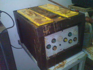
Itching Machine

 
UV light


DipTrace

Multisim

Saturday, 7 April 2012

Circuit Troubleshoot

Objectives:
  1. Troubleshoot the short circuit after do the itching process
  2. Troubleshoot the open circuit after do the itching process
  3. To prevent short circuits when soldering components 

Procedure:
  1.  After itching process is finished, testing do by to check the open circuit and short circuit.
  2. There we use a multimeter the check the circuit.
  3. On multimeter set it on 20 kilo ohm.
  4. Connect red and black prob to the multimeter. Test a meter to make sure it working.
  5. Touch the probe to the circuit and look at the indicator meter.
  6.  If the circuit is broken, the circuit should be connected by using solder.
  7. Then check the circuit again using multimeter.
  8. If the circuit in short circuit, disconnect with a knife or any material.
  9. Then check the circuit again using multimeter.
  10. Schematic circuit is used as a reference during a test
  11. Do the process until error vanish 
Analysis:

In this case, circuit we only have problems in short circuit and have no problem at open circuit. This is because, when printing on paper, sketch too close to the circuit between the connection. To solve that problem testing do and and which circuit have a short, it disconnect with a knife or any material. 

Conclusion:

Testing is very important to be done on the circuit after the itching or any wiring done at the circuit. This is to ensure that the circuit is in good condition and to avoid problems when the components is soldering. 


Test using Multimeter

Short Circuit Troubleshoot

Open Circuit Troubleshoot

Disconnect The Short Circuit

 Multimeter


Saturday, 31 March 2012

P.C.B Board Itching For The Solar System

Objective: 
  1. Preparing to construct the circuit by using P.C.B board
  2. To make the arrangement of component before make a soldering
Procedure:
  1. Photocopy the PCB layout (In Previous Report) in to  sheet using laser printer    
  2. Attach the paper on the P.C.B board. The P.C.B. board avoid exposure to light.
  3. Put transparent paper sheet and the photo-etch board into a UV exposure unit for 60 second.
  4. Wash the developing using ferric chloride. Let the P.C.B in the acid and shake it till the circuit clear from copper that not needed on a board.
  5. Transfer the PCB in to etching tank and do the operation for 4 minutes.
  6. After finish on etching tank, scrub the P.C.B board using sand paper
  7. Make sure the connection of PCB is in right continuity. 
Result and analysis:
  • All the process of producing the PCB is done step by step
  • To make sure circuit connected do the testing to circuit by using multimeter

Conclusion:
The method are used in this PCB process are essential so that no important steps are skipped. Skipping any of these may cause failure to the outcome of the project. The steps are done is to helped us troubleshoot the hardware and software if any complications should arise

  Transparent Paper 

 UV light


P.C.B board on ferric chloride  

 Etching Tank


Sunday, 25 March 2012

Preparing To P.C.B Board Entching

Objectives:
  1. To prepare the circuit before
  2. To make the P.C.B layout
  3. To confirm that p.c.b solar layout
  4. To make sure that p.c.b layout correct before do the etching

Procedure:

  1. Here we have two choice. First, design the P.C.B by using software(Diptrace). Second, by using p.c.b layout from magazine.
  2. To facilitate the design process of making p.c.b circuit layout, there are examples in the magazine was edited according to the size needed   
  3. Original size and shape to the left magazine during edit on the p.c.b circuit sizes must follow to determine what was in the magazine. This is to prevent the components such as IC can not enter.
  4. Width of the circuit that edit or sketch is 38 mm. while the circuit is 51mm long.
  5. After the editing process is made, the circuit print on the A4 paper. Double check circuit.
  6. If the circuit was not clear print, color the circuit to avoid the circuit is broken when the circuit is print on transparent
  7. After this process is complete then print paper had made ​​photocopy to the transparent paper.
  8. If there have a problem on the transparent paper repeat the process for the second time. 
conclusion:

After all this process is made and has resulted in a complete p.c.b layout and all according to what is required then the next process can be done. The process is the process of etching the solar power   circuit                              


Print from the magazine

P.C.B that print on transparent paper


Monday, 19 March 2012

Different Between Component

There we have different between  from a same component that take from the magazine and after the component buy at store of 'Jalan Pasar'. The component is transistor (in circuit TR1). Transistor's serial number from magazine is TIPP31C npn and after buy they give transistor that have serial number give is TIP31C. The problem is, that both of transistor is the same component or other type of transistor? 

Transistor TIPP31C  Datasheet.

Name: TIPP31C
Material of transistor: Si
Polarity: npn
Maximum collector power dissipation (Pc): 800mW
Maximum collector-base voltage (Ucb): 100V
Maximum collector-emitter voltage (Uce): 100V
Maximum emitter-base voltage (Ueb): 5V
Maximum collector current (Ic max): 2A
Maximum junction temperature (Tj): 150°C
Transition frequency (ft):
Collector capacitance (Cc), Pf:
Forward current transfer ratio (hFE), min/max: 20T
Manufacturer of TIPP31C transistor: TI 
Package of TIPP31C transistor: TO92
Application: Medium Power, General Purpose

Transistor TIP31C Datasheet

DESCRIPTION
The UTC TIP31C is a NPN expitaxial planar transistor,
designed for using in general purpose amplifier and switching

Collector Base Voltage:100 V
Collector to Emitter Voltage: 100 V
Emitter To Base Voltage: 5 V
Collector Current(DC) IC: 3 A
Collector Current(Pulse) IC: 5 A
Base Current: 1 A
Collector Dissipation(Tc=25°C): 40 W
Collector Dissipation(Ta=25°C):2 W
Junction Temperature Tj: 150 °C
Storage Temperature: -65 ~ +150 °C


Wednesday, 22 February 2012

Buy The Component

Objective:
  1. To search all the components and material use for project
  2. Purchasing all the material
  3. To recognize all the material that use in the project
  4. Recognize the components codes   
Procedure: 
  1. List all of solar power supply component before purchase
  2. Confirm every unit all of component 
  3. Do survey for price to the store and also from the internet.

Result and analysis:
  • All the component are purchased
  • The reason for why we have to recognize the codes of the component is to have a right component to construct the circuit 
Table of component list and price:


Component
Total
Price/RM
Resistor  180 ohm
1
0.10
Resistor 15M ohm
1
0.20
Resistor 100K ohm
1
1.30
Variable Resistor 1M ohm
1
0.50
Capacitor 1 F
1
13.00
Capacitor 470 microfarad
1
0.50
Transistor TIPP31C NPN
1
1.50
Zener diode 1W
1
0.10
Signal diode 1N4148
1
0.10
Transistor 2N3819
1
2.50
Solar Penal 6V-12V 1mW
1
28.00
P.C.B BOARD
1
10.00
TOTAL

57.7

Conclusion:


  • After finish this week of activities, we are able to understand how to read all components’ code for constructing the circuit in the right way.